ADAT modification for the Layla converters
Background and Motivation
Since this project involves a bunch of digital audio stuff that some of my readers might not be familiar with, I’ll start by describing my motivation for the project and some of the background information about the protocols and hardware involved. If you’re already familiar with this stuff and just want to see the hack, jump to the next section.
I have a somewhat unusual audio setup at home. I use a DAW (digital audio workstation) software on my desktop computer as a digital mixer for all of the sound coming from it. Using JACK on Linux, I route the output of each program to a different mixer channel, so in addition to having different volume settings for each program, I can apply effects as well (such as equalization or applying a little bit of compression when watching a movie late at night, so the loud parts aren’t quite so loud.) I can then route the audio between multiple outputs, primarily my studio monitors and my headphone amplifier.
The sound card I use is an RME Digi9652. These are older PCI cards, which are now inexpensively available second-hand since newer computers have mostly PCI-e slots instead. But, the card still works on my motherboard, has great Linux support, and provides 26 inputs and 26 outputs with very low latency. Like many multichannel audio cards, all of the I/O is digital. The 9652 has three pairs of ADAT Lightpipe ports and one pair of coaxial S/PDIF connectors. In order to get analog audio in and out, it requires the use of external converters connected to the ADAT ports.
ADAT Lightpipe is a protocol developed by Alesis in the early 90s for their digital multitrack tape recorders (the Alesis Digital Audio Tape, or ADAT). It uses the same plastic fiber optic cables and connectors as consumer TOSLINK connections, but carries 8 channels of audio rather than a stereo pair. The ADAT tape deck is now pretty much obsolete as most digital audio recording is now done with computers or hard-disk based recorders, but the optical interface is still around, often just called “ADAT” now. The relatively low complexity of its implementation and inexpensive LED transceivers has established it as the de facto standard for connecting low channel count digital audio devices together.
Previously in my home setup, I wasn’t using any of the inputs, and ran 4 channels of output—two to my headphone amplifier and two to my monitors. I was using another board that I built (which I might write about later) to take one of the ADAT outputs and split it into multiple 2-channel S/PDIF outputs, one of which went to a Benchmark DAC1 driving my headphone amplifier and the other to my AMB γ2 driving the monitors.
I wanted, however, to be able to include some of my other audio devices in the same setup as well. One of these devices is my Netflix player; I run Linux on my desktop which Netflix doesn’t support, so it’s easier just to use hardware where it’s supported. Basically, I wanted a few analog inputs that I could plug other devices like this into in order to get their audio into my mixer, so it could be processed and routed like the audio coming from software running on my computer.
The Hack
The off-the-shelf solution to my problem would have been to just buy an 8-channel A/D and D/A converter box with ADAT I/O. These tend to start somewhere around $500 for a cheap one, though, and I didn’t want to spend that much. They also tend to hold more of their value second-hand, as ADAT is still widely used, so it’s harder to find cheap used ones. But, there was something interesting in my junk pile that ended up being the solution.
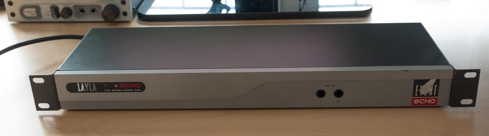
This thing is the converter box for an audio interface that Echo made in the late 90s, called the Layla. There were two other audio interfaces in the Event series, named Darla and Gina, with fewer channels—the Layla was the top of the series with 10 analog outputs and 8 analog inputs. It connected to the computer by a 25-pin proprietary umbilical cable to a PCI card. I came across this interface box being thrown away, with the PCI card long gone. By itself, it’s practically worthless, as the 25-pin interface is not at all standard. I originally grabbed it intending to salvage some of the parts out of it and maybe re-use the case (empty rackmount cases are expensive!)
But my current need for audio I/O had me looking at it again. I decided to replace the DB-25 connector with an ADAT interface, which would let me connect it to my RME card. I’ll jump to the end result and show it working before I go into detail on how it was done:
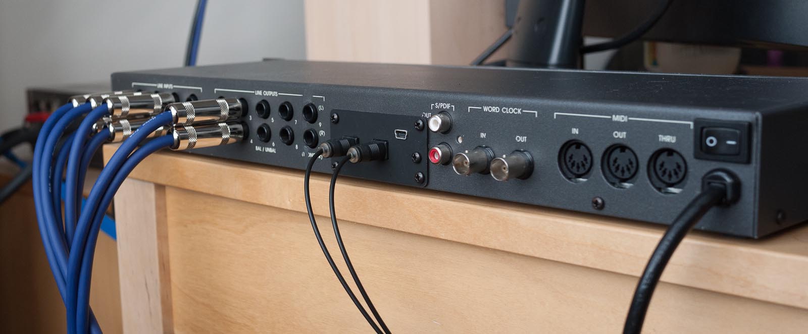
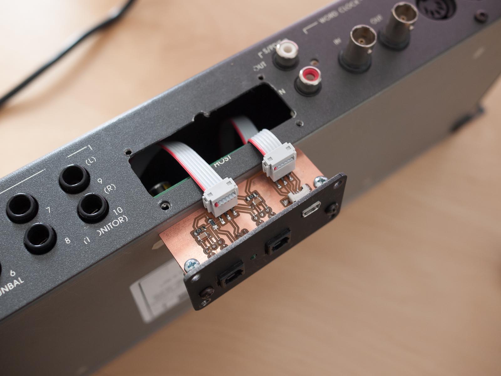
That black plate in the middle is the only indication that it’s been modified. It covers up the spot where the original DB-25 connector was, and replaces it with a pair of optical connectors and a mini USB port for configuration. On the left side are the analog inputs and outputs; these are all functional except for outputs 9 and 10 (as ADAT only carries 8 channels). The wordclock I/O is also functional, though the S/PDIF and MIDI are not.
To accomplish this, I essentially re-used the whole analog section and the converters themselves, while re-wiring and replacing most of the digital electronics. Inside
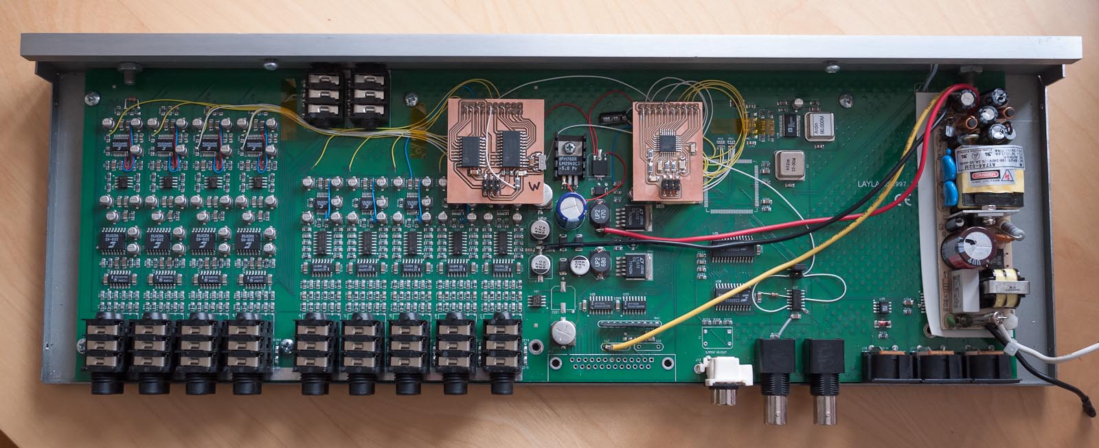
Inside the Layla box (ignore the modifications for now) the analog inputs are the section on the left, and the outputs are immediately to the right of the inputs. Both directions use Crystal Semiconductor (now Cirrus Logic) converter chips, with two channels of audio handled by each chip. On the input side, there’s an MC33079 op amp acting as a balanced line receiver, a CS3310 digital volume control IC, and another op amp buffering the inputs to the CS5335 analog-to digital converters. The CS3310s are controlled over a serial (SPI) bus, and allow the input gain to be set anywhere from -95.5dB up to +31.5dB, in 0.5dB increments.
On the outputs, the CS4327 converters feed into more MC33079 op amps that act as the balanced line drivers. Each pair of channels also has a quad CMOS switch, with two switches allocated to each channel. One disconnects the converters from the line drivers, acting as a hardware mute. The other switches an extra resistor into the feedback loop of the op amps, dropping the output levels from +4dBu to -10dBV.
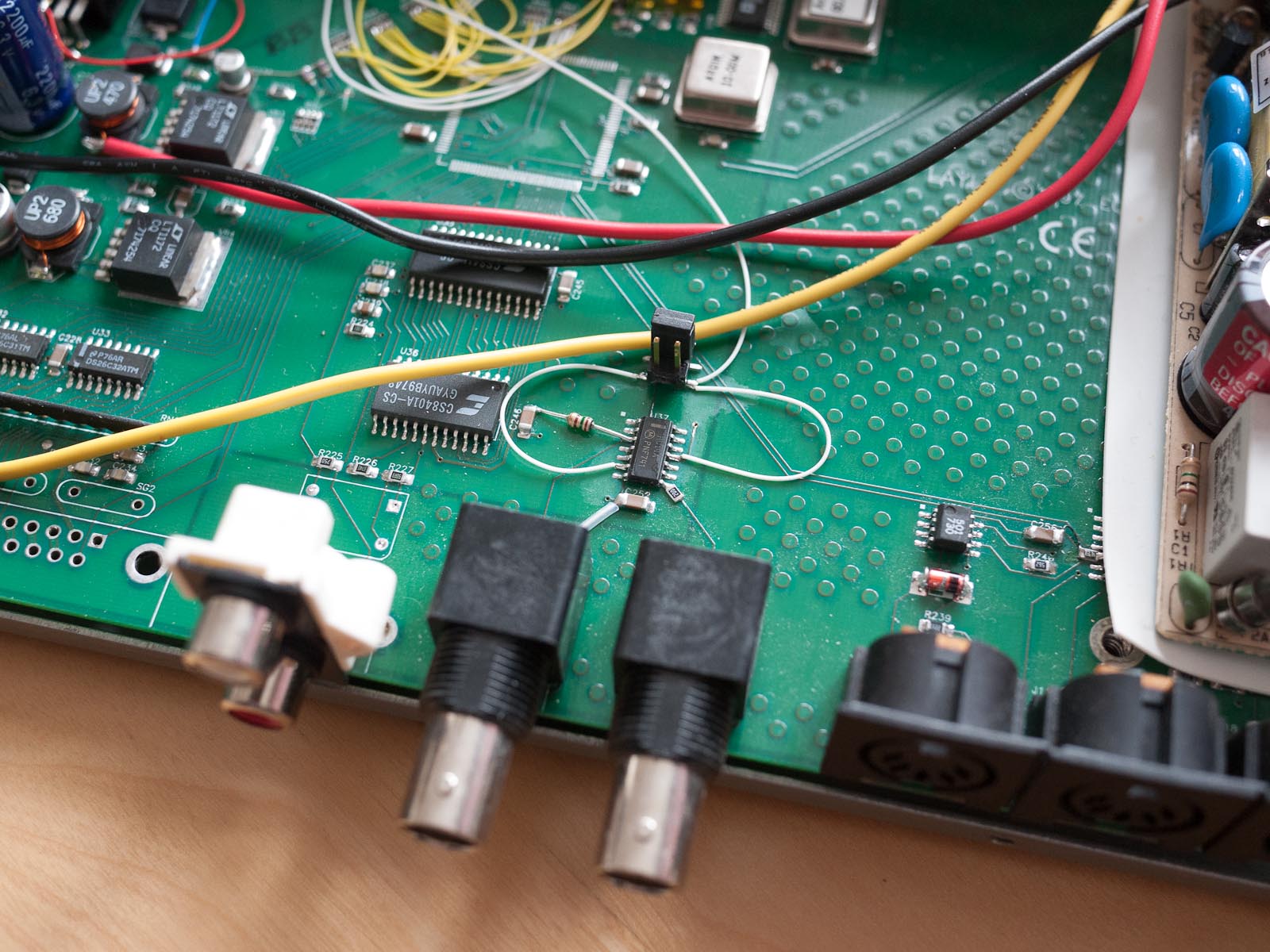
To the right of the outputs is the power supply, which creates the ±15V analog voltage supply rails for the op amps, and the +5V analog/digital supply for the converters and digital volume controls. The big red, black, and yellow wires are actually how it came from the factory—originally, Echo intended to power the interface box from the PCI card (you can see where the 25-pin connector used to be below the power supply, by the way) but they ended up adding the dedicated power supply stuck on to the right side of the board after being unsatisfied with the performance of the device when it was running on noisy computer power at the end of a long cable that also carried high-speed digital signals. [1]
To the right of the power supply, there used to be an FPGA that coordinated all of the converters and sent the data back over the 25-pin cable. In the picture above, I’ve removed the original FPGA completely.
The modification consists of two main parts: the ADAT interface itself, and a microcontroller to manage the digital controls like the input and output gains. ADAT Interface
ADAT Lightpipe was covered by a few patents that Alesis owned, which meant paying license fees to include it as an interface. As a result, there aren’t a lot of off-the-shelf chips that handle ADAT. (This is now changing—best I can tell (though I am not a lawyer) the patents have recently expired, and implementations of the ADAT protocol are now showing up as IP blocks that can run on FPGAs and some microcontrollers.) For this project, I’ve used the Wavefront chipset. Wavefront Semiconductor manufactured a couple of Alesis’s custom chips, including the AL1401AG and AL1402G ADAT interface chips. These are presumably the chips that were inside the actual ADAT decks (though I’ve never taken one apart to confirm that).
The AL1402G takes an ADAT bitstream and decodes it into 4 channels of serial digital audio, with each data line containing interleaved data for two audio channels. It also recovers a system clock (256Fs, where Fs is the sample rate), a bit clock (64Fs) which indicates when the individual bits of audio data should be latched, and word clock (Fs). The AL1401AG takes the serial audio signals and wordclock and goes the other direction, producing an ADAT bitstream.
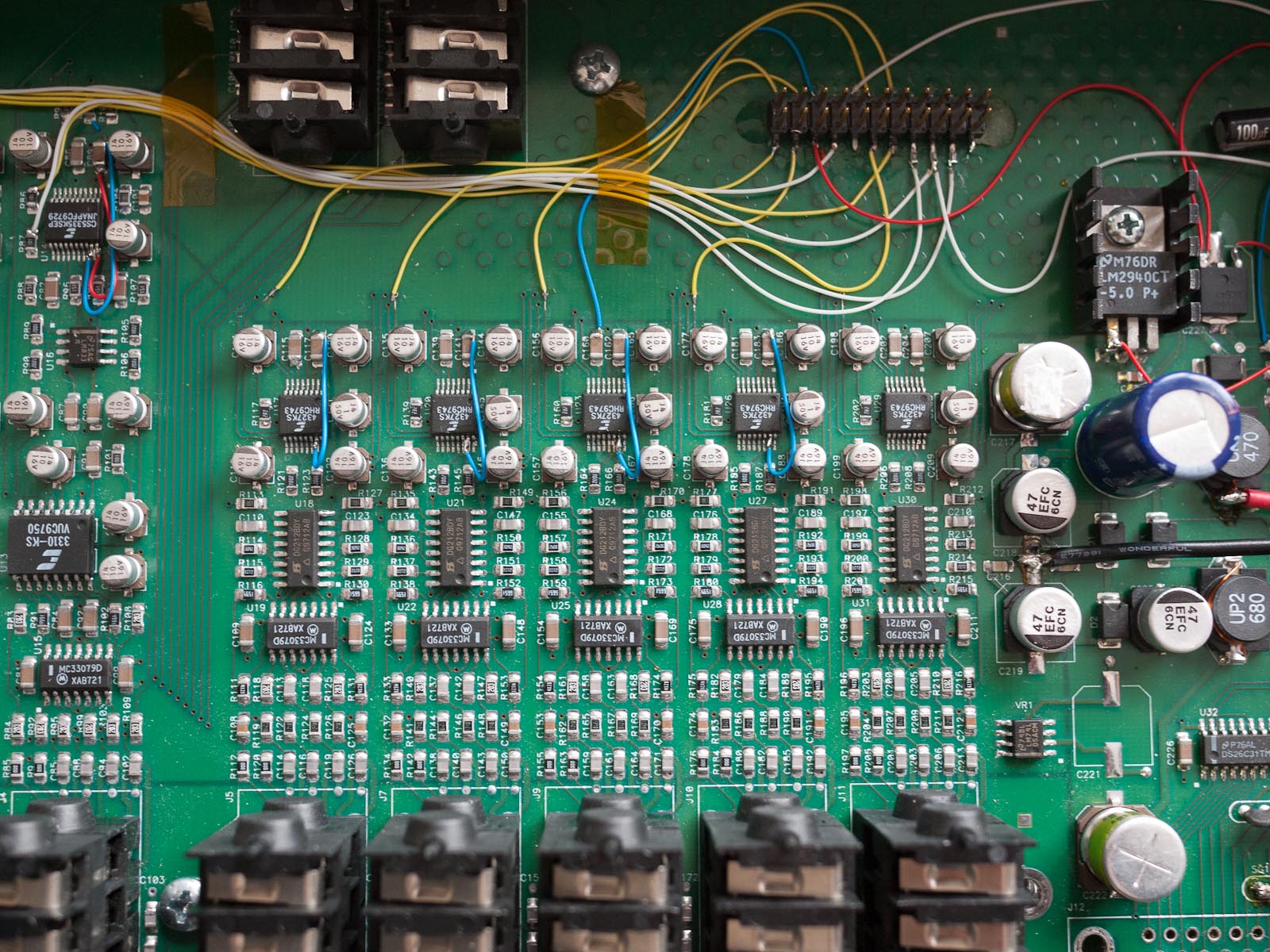
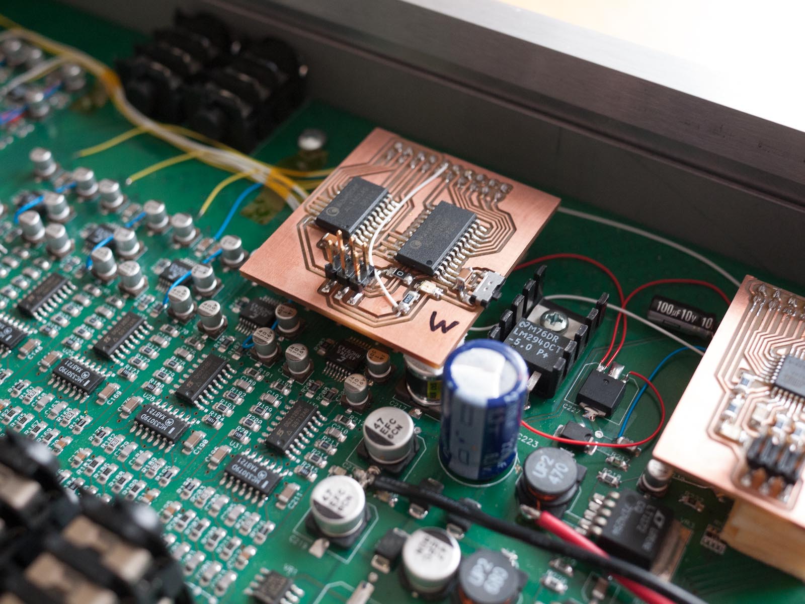
To add the ADAT chipset, I started by gluing a 20-pin header to an open space on the board. I glue the headers down first with superglue, and add some 2-part epoxy later to really make sure that they stay put. This provides a point from which signals on the board can be wired into an additional PCB that can be easily disconnected for servicing.
The signals are then wired up using 30-gauge wire-wrapping wire. I’ve roughly color-coded data lines as yellow, clocks as white, power as red, and ground as blue. The various signals were located by referencing the datasheets for the converter chips and looking for continuity between the pins on the chip and easier places to solder to. The A/D converters have resistors on most of their signals, which have nice big pads to which to solder wires. The D/As didn’t have the resistors on the data lines, so I’ve scraped away a bit of the soldermask on the traces and soldered the wires to the exposed copper. The clock lines are shared between all of the converters on the board, so the clock signals just connect in one location and then run through the traces on the PCB to everything else. I did cut off the part of the traces where they used to run to the FPGA to keep them from acting as big antennas.
There are a couple of different formats for serial digital audio—they all use a system clock, bit clock, and word clock (sometimes also called LR clock because its value toggles between the left and right channels) and all will generally have 32 bits of data transmitted for each channel. Most audio converters are either 16, 20, or 24-bits, however, so there’s variation on which of those 32 bits are used to transmit the actual data. The two most common are left-justified (where, for a 24-bit converter, the first 24 bits are used and the last 8 are ignored) and I²S, which is like left-justified but the first bit of the channel comes one bit clock cycle after the word clock changes, rather than at the same time. Right-justified formats are also sometimes used as well. To account for all of these different formats, most chips that have a serial digital audio interface have a couple of pins that can be set high or low to configure which format should be used. This is true of both the converters in the Layla and the Wavefront chips. Unfortunately, the Layla PCB is hardwired to configure the converters to use I²S, which is a format that the Wavefront chips don’t support. This required lifting the configuration pins off of their pads on the PCB and running short wires to connect them to either power or ground. With the D/A converters, it was only necessary to change one of the configuration pins, which you can see as the short blue wires next to the chips. On the A/D side, both configuration pins needed to change, so there’s both a red and a blue wire. Wiring-wise, this was the most tedious part of the modification.
The actual board that carries the ADAT chipset is made from a single-sided PCB, with the spaces between traces milled out with a 1/64″ endmill. A 20-pin through-hole connector on the back side of the board mates with the 20-pin header epoxied to the original board. The ADAT transceivers connect via the 6-pin header on the top side of the board, which will be discussed later in this article.
Next to the ADAT board, you can also see an additional 7805 regulator that I’ve added to the main PCB. The existing 5-volt supply is already pretty heavily loaded by the converters themselves, and since it’s also used by the analog side of the converters, I didn’t want to put too much more digital circuitry on it. The additional 7805 is a separate supply that runs the circuitry I’ve added. The tab is soldered to a pad for an electrolytic capacitor that was unpopulated on the original board.
The Controller
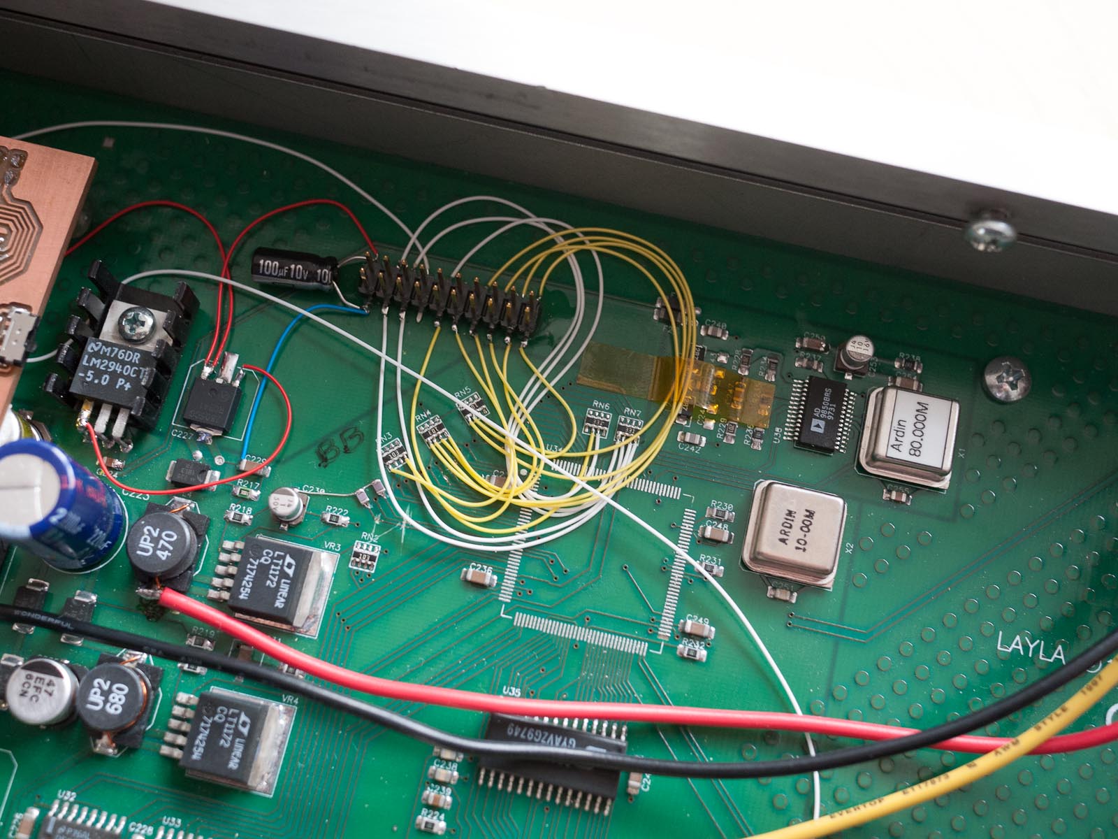
The original Layla came with software that allowed the user to adjust the input and output gains. This was mediated by the FPGA, which I removed. To be able to control these signals, I added another 20-pin header and PCB that controls these signals. I used an ATmega32U2 microcontroller, which has just enough I/O pins for the task. The 32U2 also has a USB interface, with which I provide a way for the settings to be changed from a computer.
All of the digital control lines conveniently come out to resistor packs near where the FPGA used to be. There are 4 chip select lines for the 4 digital volume ICs, as well as shared clock and data lines for their SPI bus. Then there are 9 digital lines that go to the CMOS switches on the output—8 switch the individual outputs between +4dBu and -10dBV levels, and the ninth is the mute signal, which applies to all channels at once. The controller board connects to these lines via the epoxied header, and the USB port on the back panel connects through another 6-pin header on the top side of the board.
The USB port, when connected, shows up as a vendor-specific USB device, for which I’ve written a small command-line tool in Python that allows changing the gains. The actual gain settings are stored in the microcontroller’s EEPROM, so they are retained across power cycles.
The error signal from the ADAT receiver is also wired to the microcontroller, which drives the mute line when no ADAT signal or an invalid ADAT signal is present. This prevents horrible noises from going to the outputs when the ADAT input is unplugged. The D/A converters don’t have any kind of built-in muting feature, and have a tendency to produce very loud squealing noises if the clock inputs are invalid. The automatic muting keeps that noise from going to my speakers.
The Rear Panel
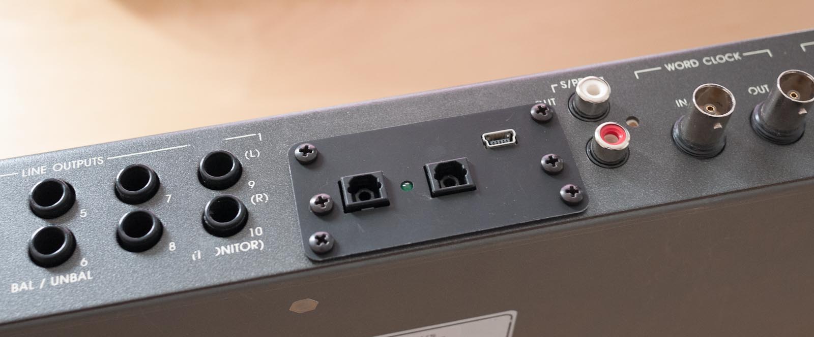
The actual connectors are mounted on the back of the case on an aluminum plate. The optical transmitter and receiver were salvaged from a lightning-damaged AudioBox 1818VSL (long story.) There’s also an LED on the back panel that lights up when a valid ADAT bitstream is present on the input, and the USB port for controlling the gains.
The panel is waterjet-cut from 1/16″ aluminum and somewhat hastily spraypainted matte black. A small PCB with the I/O connectors screws on with a pair of angle brackets.
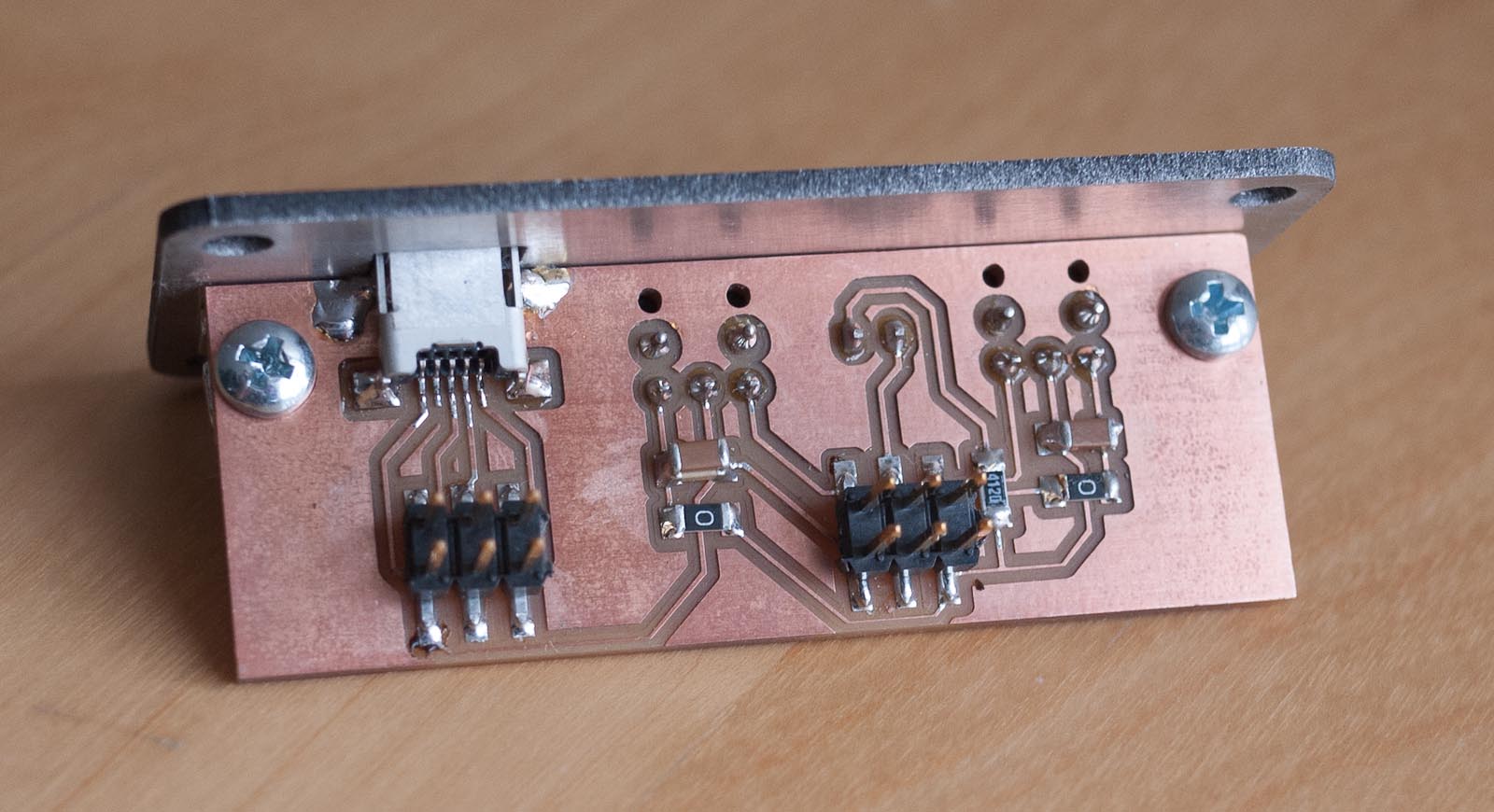
The optical transmitter and receiver are through-hole parts, so they end up on the other side of the single-sided copper board with the LED and brackets:
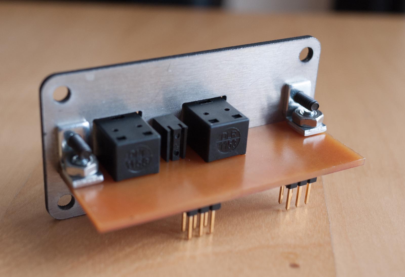
And then everything gets connected together with 6-pin ribbon cables, through a hole milled into the back of the box where the original DB-25 connector used to be:
Clocking
I wanted to be able to still use the wordclock input and output on the back of the box—wordclock is always useful to have in larger audio systems. The clock recovered from the ADAT bitstream is also sometimes more jittery than desirable. The ADAT receiver chip supports a wordclock input as well.
The clock configuration isn’t as cleanly done in this hack at this point, mainly because I didn’t have a digital mux in my parts bin that would have enabled the microcontroller to select the clock source. Instead, the ADAT receiver can be switched between clock modes with the little slide switch on the side of the ADAT board, and the buffered signal from the BNC jack is enabled with this jumper on a header (also glued to the original PCB):
So, currently, changing the clock source requires opening up the case. I might at some point get around to adding that mux so it’s software selectable.
The wordclock output connector is always active, and will output whatever clock source the board is currently using. Conclusion
In the end, it works great! It ended up being a bit more work than I was expecting (especially discovering that the config pins on the converters were going to need to get lifted from the baord to change the data format) but it’s always nice to recycle something useless into something functional. The entire hack took a couple days, starting with probing for the signals, adding the headers and soldering all of the jumper wires, making the PCBs, debugging, testing, and finally writing the software for the microcontroller (which I’m still tweaking a little bit.)
The converters are old—they are only 20 bits whereas most newer pro audio gear is 24-bit, but 20 bits is actually fine for most purposes. The analog stuff is actually pretty well done, and I’m pleased with how it sounds. I haven’t tried it for any serious recording work (yet), but the outputs are actually very satisfying on my monitors, which frees up my gamma 2 DAC for me to use elsewhere.